
Published Oct. 6, 2026. Applied Materials and Intel have announced an expanded research collaboration focused on chipmaking technologies for artificial-intelligence computing, including next-generation transistors, advanced interconnects and 3D packaging.
The companies said the work will connect research teams at Applied Materials’ new EPIC Center in Silicon Valley with Intel’s research and development campus in Hillsboro, Oregon. Their stated goal is to shorten the path from laboratory development to high-volume manufacturing in the United States.
What the collaboration covers
According to Applied Materials’ Oct. 6 announcement, the joint program spans materials, process technologies and device architectures for advanced logic nodes aimed at AI workloads.
The work includes front-end transistor development, back-end interconnect scaling and packaging research tied to Intel’s Foveros 3D-stacking platform. Those packaging efforts are intended to increase connection density while improving power delivery and heat management in high-performance computing systems.
Applied Materials described Intel as a founding partner at the EPIC Center. The facility is scheduled to become operationally ready in 2026 and is designed to let equipment suppliers and chipmakers test manufacturing processes together earlier in the development cycle.
Why advanced packaging matters
AI systems increasingly combine several specialized computing and memory components rather than relying on a single large chip. Advanced packaging connects those components at high speed, but it also creates difficult power, heat and manufacturing challenges.
Closer collaboration can help equipment makers and chip manufacturers identify those problems before a process reaches a production line. The announcement does not identify a specific chip launch, factory schedule or financial commitment, however, and the claimed development benefits remain forward-looking.
What to watch next
The practical test will be whether the partners disclose measurable manufacturing milestones, customer adoption or new products that use the jointly developed processes. Applied Materials said the collaboration is intended to improve the speed of technology transfer into high-volume manufacturing, while Intel linked the effort to its foundry and U.S. manufacturing strategy.
The partnership arrives as power availability and infrastructure have become central constraints on AI expansion. AskNovus recently reported on Google and Constellation’s 3.59-gigawatt electricity agreement, while device users can also follow the latest Android and Samsung security updates.
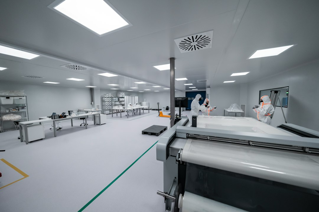
Featured image: Photo by TECNIC Bioprocess Solutions on Unsplash. Image is illustrative.
[…] production. It follows other large technology-manufacturing investments, including the recent Applied Materials and Intel research partnership. Readers can follow additional company developments in AskNovus […]